


Scientific Exchanges
March - August, 2016: Pawel Czaja
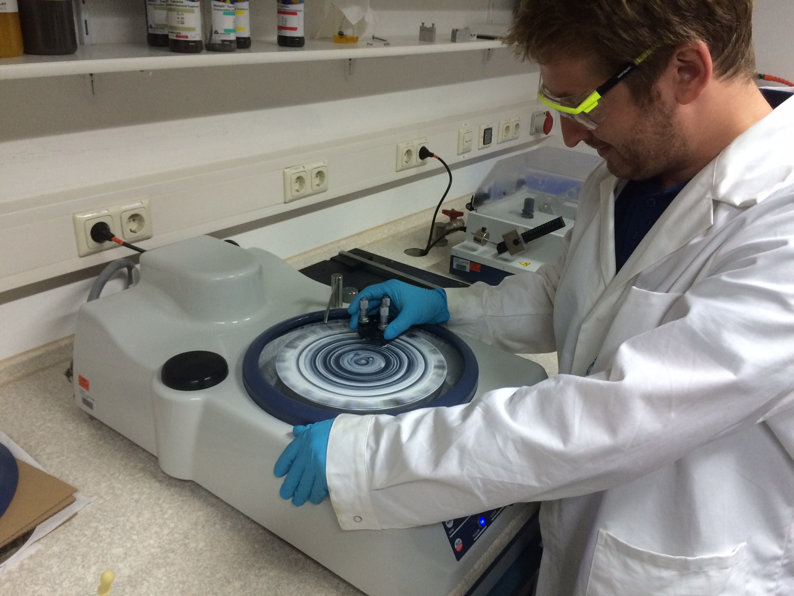
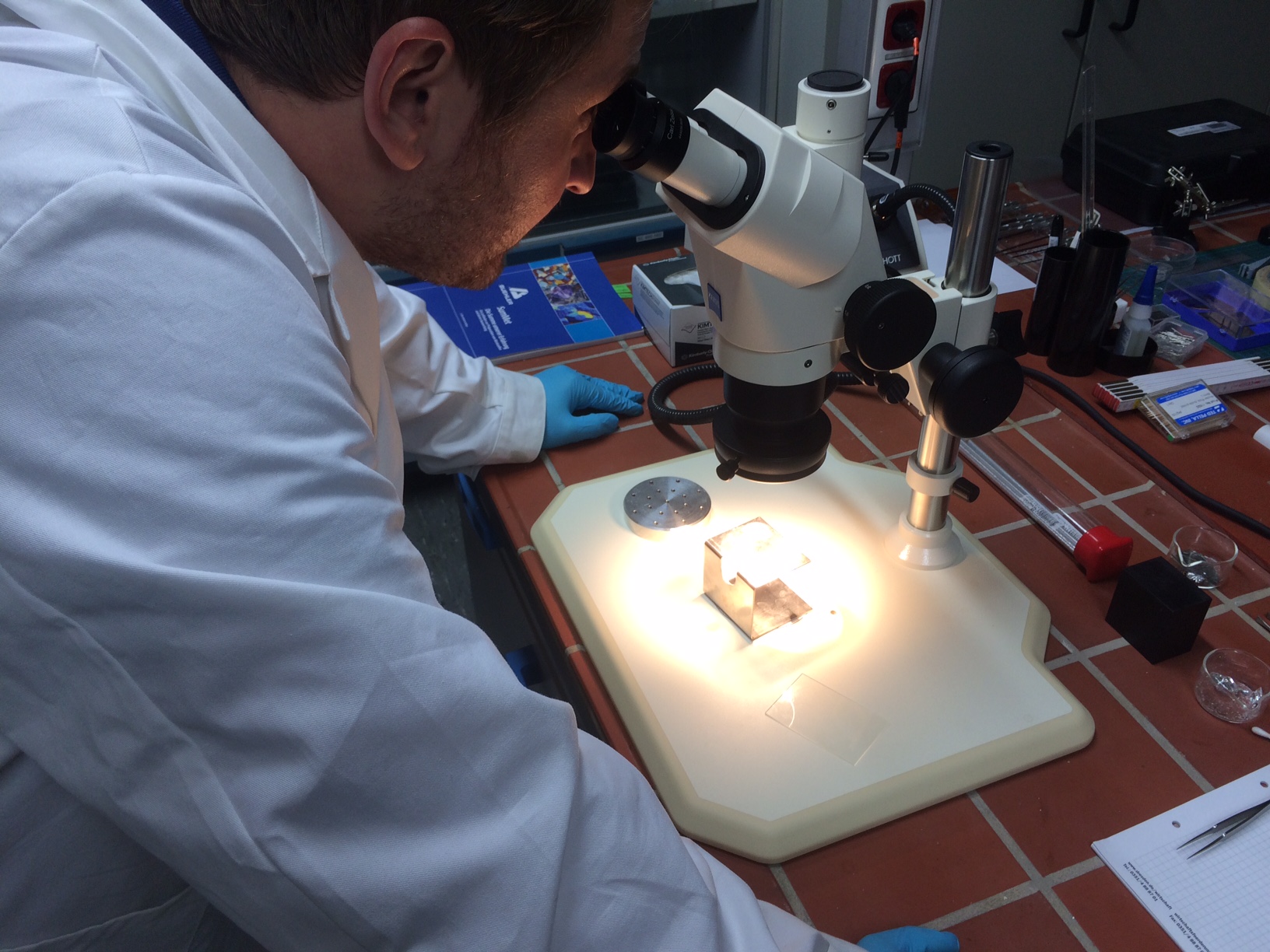
My research interest comprise magnetic shape memory alloys, which are a unique class of „smart” materials capable to provide response to an external stimuli such as to changes in temperature, stress or magnetic field. The underlying phenomenon of this exceptional behaviour is related to the coupling between structure and magnetism, which is further associated with a reversible martensitic phase transition. This transition is a solid to solid, thermoelastic phase change between two iso-chemical polymorphs with distinct differences in structural and magnetic properties. The magneto-structural coupling leads to a variety of fascinating and complex physical phenomena including giant magnetic field induced strain, giant magnetoresistance, giant magnetocaloric effect etc., which render these systems highly interesting for variety of applications in smart materials technology (e.g. actuation, sensing, magnetic cooling, energy harvesting).
An important consideration in studying and developing the functional properties of magnetic shape memory alloys is the analysis of magnetic microstructure. This is motivated by the fact that domain patterns form the mesoscopic link to macroscopic properties of magnetic materials. Therefore detailed investigation of magnetic domains arrangement, their dynamics is indispensable for better understating and more effective control of many of functional properties of magnetic shape memory alloys.
The Dresden Fellowship scheme provided me with a wonderful opportunity and means to enter this extraordinary and aesthetically beautiful world of magnetic domains and their structures. Except from looking into magnetic domains we have also studied by use of TEM precursor phenomena preceding the onset of the martensitic phase transition in Ni-Mn-Sn Heusler alloy belonging to the family of magnetic shape memory alloys. Some attention was also given to the microstructure of novel metal-ceramic composite material with some potential for automotive and aviation industry. I had access to fantastic and highly capable scientific instruments including scanning and transmission electron microscopes, polarised light microscopes, X-ray microtomography, great facilities for sample preparation and ever willing, well skilled staff who has never offered me help without a smile.
Throughout my stay I gathered an abundance of scientific data, most of which are without precedence in state of the art literature on the subject and no doubt it will bring scientific publications increasing the visibility of DCN among the considerable shape memory alloys community worldwide. This however would not be possible without interaction with the Fraunhofer Institute (IKTS) and Leibnitz Institute for Solid State and Materials Research Dresden (IFW), where I am particularly indebted to prof. Rudolf Schaefer one of the luminaries in the magnetic domains’ universe.
One of the goals of the Dresden Fellowship is to foster and stimulate the collaboration between the host organisation and the visiting researcher’s workplace. Taking into account that plans for future collaboration and joint German-Polish projects, now at the end of my stay, are coming down the pipeline I am convinced that this goal has been achieved and I will enjoy more productive interaction with DCN, IFW, IKTS in the future to come.
As well as on scientific it was equally great and very educating experience on a human level too, since I was able to interact with a multinational team of researchers and function at the core of a well organised and exceptionally effective group. At this point I would like to take the opportunity and express my hearty thanks to all the colleagues and staff who supported me throughout my stay not only professionally but also with friendly and comfortable atmosphere, which made it for a pleasant environment to work in.
My special thanks are reserved for prof. Ehrenfried Zschech, who is a great mentor and science enthusiast and above all an inspiring researcher.
October - Dezember, 2015: Ewa Bulska
Ewa Bulska (Faculty of Chemistry, Warsaw University of Technology)
From October 2015 to the end of December 2015 I had the possibility to be on a fellowship of TUD at the Dresden Center for Nanoanalysis (DCN). My main cooperation partner at the TUD was Professor Ehrenfried Zschech. During my stay in Dresden we were working on the characterisation of various type of solids, namely on the hierarchical materials. We performed preliminary examination by SEM (the most advance model of SEM instrumentation, allocated at the Barkhausen building, (Helmholtzstraße 18) of the structure and elemental composition of the samples, e.g. bones and alloys, the samples which were preliminary characterised at my home institution University of Warsaw. During my stay in Dresden I was performing measurements together with Prof. Zschech’s PhD student Maria Aranzazu Garitagoitia. The investigation will be continued, and the draft manuscript for a common publication in a peer-reviewed journal was written.
We did start working on a common publication related to the characterisation and imagining the plant tissues towards the investigation of the distribution and the transportation of various bio-active elements. The work is in progress, and it is plan that the paper will be submitted till the end of March 2016.
A good example of the common work is that we did start working on the review paper, which is focused on the use of various imaging techniques for the characterisation of solids, their analytical performance, advantages and limitation with the examples of various solids. This work is in progress, still need more work on the bibliography and will be completed, as planned, till the end of June, 2016.
During my stay I gave presentation in two seminars. In the first one on 27.20.2015, I presented my work, experience and the possible topics which could be of interest for further collaboration; in the second one on 11.11.2015, the topic was devoted to the investigation of archaeological objects by various instrumental techniques.
Knowing the strong involvement of Prof. E. Zschech with the Fraunhofer Institute for Ceramic Technologies and Systems IKTS, I was able to visit the Institute, met a number of scientists and discussed possible fields of collaboration.
Besides my main contact with Prof. E. Zschech, I was also interacting with Prof. Karol Kozak from Medical Faculty at TU Dresden, with whom we are planning to work on the various materials which could be used for medical purposes.
During my stay I also took the opportunity to visit Leipzig, where I spent some time in the beginning of my scientific carrier (80th of last century), obtaining the fellowship at the laboratory of Professor Klaus Dittrich at the Karl-Marx Universitat, I took the opportunity to visit my colleagues in Leipzig.
Definitely I was impressed about the laboratory at DNC at TUD and its new instrumentation, which could be used by various scientific group from Dresden. I was lucky to have the possibility to perform measurements with my samples, which I brought with me. This is in my view the strength of TUD, it established a well equipment laboratory, which attract others to join. I appreciate the management support and the scientific discussions with Prof. Zschech.
In my view the most important is to intensify the exchange of faculty members, also those from the administration, which should be of benefit especially when the new international joint research projects are in a preparation stage. I also strongly believe that joined cultural programs, where staff members and students are engaged would be of mutual benefits not only for both universities but also for regional cooperation.
March - May, 2015: Anna Kaya Lewandowska
Anna Lewandowska (Faculty of Material Science and Engineering, Warsaw University of Technology)
From March 2015 to the end of June 2015 I had the possibility to be on an internship in the Dresden Center forNanoanalysis (DCN). The internship was a part of NanoMat project, established on Faculty of Material Science and Engineering at Warsaw University of Technology. DCN was chosen by me as a host institution because of its high experience in 3D material analysis and high quality of laboratories. During my stay I made X-ray tomographies of Molten Carbonate Fuel Cell components using ZEISS Xradia Versa. The tomographies of both electrodes (the anode and the cathode) were done and also new cathode components were investigated. For further image postprocessing software like Aviso or Mimics were used. The result of my work is a 3D analysis of the components. Also 3D geometrical models were created. Obtained result are important for further research on improving material components for MCFC.
In my opinion the internship in DCN in TU Dresden was very successful. I did experiments which will be further used in my PhD thesis. I had the possibility to broaden my knowledge in the field of 3D material tomography. I also gained valuable experience working in international team.
October- December, 2014: Katarzyna Berent
Katarzyna Berent (Institute of Metallurgy and Materials Science, Polish Academy of Sciences, Krakow, Poland)
Mainly I collaborated with prof. Ehrenfried Zschech, Dr. Markus Löffler and Sayanti Banerjee. The subject of my work was focused on the characterization of silicon and germanium nanowires. Using high resolution focused ion beam scanning electron microscopy (FIB-SEM FEI Helios NanoLab 650) we studied Si and Ge NWs, they have been also investigated for their application in nanoelectronic devices. The formation of single-crystalline Si nanowire heterostructure by the solid-state reaction between a Si nanowire and Ni contact pads was studied. We analyzed the strain induced Si-NiSi2 nanowires with transmission electron microscopy (TEM) and energy-dispersive X-ray spectroscopy (EDX). The next step, as originally proposed, we measured the crystallographic orientation of nanowires using HR-TEM. I also had the pleasure to work with scientists from Fraunhofer Institute for Ceramic Technologies and Systems (IKTS) in Dresden. An understanding of the atomic-scale chemistry that governs semiconductor nanowire growth is crucial for the precise control of nanoscale physical properties, especially for electronic applications. Therefore, the next step will be in situ TEM studies of Si nanowires. In situ TEM is a powerful tool for the study the growth process, reaction mechanism and thereby to control the dimension of the Si region, the potential gate of a Si nanowire transistor. The following joint research will be carried out in the laboratory of Analytical Electron Microscopy at the Institute of Metallurgy and Materials Science of Polish Academy of Sciences in Krakow. The collaboration between DCN and IMIM PAS will involve exchange and analysis of data on TEM experiments. The results of our collaboration will be published in scientific journals.
June/July, 2014: Malgorzata Lewandowska
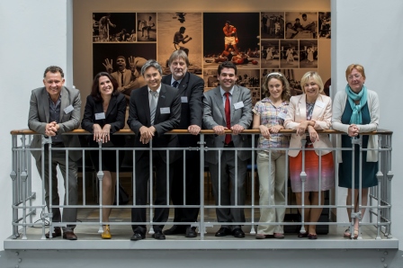
Malgorzata Lewandowska with other Fellows and the Rector of the TU Dresden, Prof. Dr.-Ing. Hans Müller-Steinhagen (left picture) and with Gerhard Rödel (Vice-Rector for Research of the TU Dresden) (right picture)
Malgorzata Lewandowska – professor at the Faculty of Materials Science and Engineering of Warsaw University of Technology, Poland.
She was a guest scientist at the DCN from June to July 2014. Her scientific interest is focused on ultrafine grained and nano-crystalline materials. The goal of her research stay was to establish a closer collaboration between the Warsaw University of Technology - Faculty of Materials Science and Engineering - and the Technische Universität Dresden - Dresden Center for Nanoanalysis - in the field of nanostructured materials and their characterization applying advanced analysis techniques including high-resolution electron microscopy and X-ray microscopy. Nanostructured materials have attracted significant scientific interest due to their superior mechanical and physical properties. They are prospective for a number of applications, including leading-edge electronic industry. Particularly, the microstructure of advanced on-chip interconnects has to be engineered to fulfil performance and reliability requirements for advanced electronic products. For this field of research highly sophisticated materials analysis techniques are needed, e. g. high-resolution electron microscopy and X-ray microscopy to understand microstructural factors influencing the properties of nanostructured materials.
March/April, 2014: Agustín R. González-Elipe
Agustín R. González-Elipe - professor at the Nanotechnology on Surfaces Laboratory of the Institute of Materials Science of Sevilla, Spain.
The strategic goal of this stay is to establish a closer collaboration between the Nanotechnology on Surfaces Laboratory of the Institute of Materials Science of Sevilla (ICMSE, joined center between the CSIC and the University of Sevilla) and the Dresden Center for Nanoanalysis at Technische Universität Dresden. This collaboration should pave the way for a long term cooperation between the two centers in view of other more ambitious initiatives and common research in the field of advanced materials. Both Institutes are quite committed in the development and characterization of nanomaterials aimed for a wide range of functional applications. In this context, not only the synthesis and the processing of the materials are of the outmost importance, but also their characterization at nanometric and even atomic scales. In fact, in the field of research of nanomaterials highly sophisticated analysis techniques (e. g. high-resolution electron microscopy, scanning probe microscopies or X-ray microscopy) are needed to unravel their structure, microstructure and properties, all of them related with the intimate organization of matter at nanometric scale.